This design note presents a phase-locked control loop for a brushless DC (BLDC) motor using the TI DRV10866 driver chip. The implementation is executed in an FPGA. This is part I of a two part series; Part II is here.
Part I
In the overall system the once-around signal Fg/6 is phase locked to an external reference Fref. The Fg signal is available as an output on the DRV10866 motor driver.
Inner Loop Structure
The inner loop is a frequency locked loop using lead-lag compensation. A system block diagram for the loop is shown in Figure 1 using a Phase-Frequency Detector (PFD). In steady state the PWM value is the finite (non-zero) value needed to command the motor torque. Likewise, the output of the compensator needs to be a non-zero-value to generate the steady state torque. If the steady state maximum phase error of the PFD is not enough to provide the running torque the system will not achieve frequency lock. (Note: click figures to see a high resolution view).
Figure 1 - Control Loop for BLDC

The DRV10866 driver chip by itself does not provide any speed control of the motor. The input is a pulse-width-modulated (PWM) logic signal that provides a 5V peak trapezoidal voltage to the motor. The motor speed will change with voltage, temperature, windage and load. Feedback control is needed for accurate speed control. Phase locking drives the speed error to zero.
The DRV10866 driver is being considered over the DRV10964 because the DRV10964 a LPF (~4.2Hz) cascaded with the PWM input. This adds an extra pole in the system close to the region of control interest.
Motor & Driver Parameters
The BLDC motor example here is typical of a 2.5in HDD motor. It is a 3-phase brushless and sensorless. The input to the driver is a PWM logic signal and the output is a logic signal Fg which has a frequency related to the motor RPM by the following relationship, given the control logic input FGS:
- FGS logic 0:
- FGS logic 1:


Where Npp is the # of pole-pair
The first task is to derive the small signal transfer function from PWM to Fg to design the controller H[z] and properly scale the FPGA control registers.
The nominal motor parameters are defined in Table 1.
Table 1 - Motor parameters

Motor & Driver Block Diagram
A control block diagram of the motor and driver is shown in figure 2. This includes the electrical and mechanical parameters of the motor and assumes the winding commutation is handled optimally.
Figure 2 - Motor & Driver block diagram

The drive voltage to the winding is a trapezoid with peak scaled to the PWM duty cycle. If the PWM duty cycle is a fraction in the range [0 1] then the trapezoid is (pwm) * Vc peak voltage. The other parameters of the block diagram are given in Table 1. The input pwm is digitized to 9 bits and filtered with a low-pass filter
The linearized transfer function from the driver input to Fg in the continuous s-domain is given by Equation 1.
Equation 1:

where Jt == Jm + JL.
This can be converted to the discrete z-domain using the appropriate zero-order hold conversion. Note the sampling frequency for the inner loop is Fg ~= 360 Hz which limits the allowable open loop bandwidth. For the values given in Table 1 and with Fg= 360Hz the bode Hd(z) is shown in Figure 3.
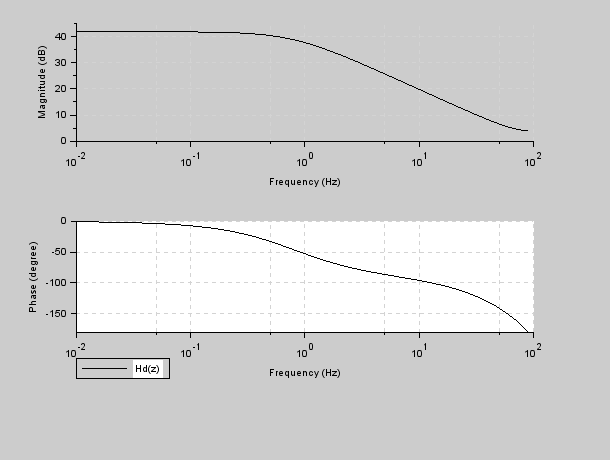
Figure 3 BLDC Bode plot
FPGA Compensation Logic
A block diagram of the loop compensator and phase detector is shown in Figure 4.

This shows a phase detector, Kpd, with a limiter on the phase error. The limited error drives a phase lead-lag compensation block with a cascade gain Ko. This is followed by a conversion to a variable duty cycle pwm signal with gain Kpwm. This can be written as a z-domain gain from (Fref-Fg) to pwm as follows:
Equation 2:

The overall transfer function of the BLDC plus driver and FPGA compensation will be the cascade of the above two transfer functions when both are represented in the discrete z-domain. The FPGA block has two poles at z=1 and z=b and a zero at z = a. The design parameters of the FPGA will be register values to achieve the coefficients Ko, a and b.
The motor-driver transfer function from pwm to Fg is Type 0 with a low frequency pole from damping and a high frequency pole due to the electrical L/R time constant. There is also an additional pole due to the pwm low-pass filter built into the DRV10964, which is why I’m using the DRV10866. The zero of the compensator is required for the system to have a stable gain with adequate phase margin.
Details on FPGA Compensation
This section gives some detail on implementing the compensation in FPGA logic. The transfer function of the compensation alone is given in equation 3.
Equation 3:

Given the input signal at discrete times is err(k) and the output signal is y(k) the difference equation for the compensation is

The values at time k-1 are the previous values that were stored on the previous calculation. The values at time k are the current values either measured or calculated at time k. The coefficients a and b are 0< and <1. These are represented in the FPGA as a fraction. As example 61/64 is 0.953125. The denominator 64 is a signed right shift by 6 bits which is represented as ‘value >>> 6’ in the Verilog code. If the integer numerators are given by a, b and Ko the difference equation can be written as shown here.

The difference equation is computed in the FPGA using a pipeline to store intermediate values used in later steps. Refer to the bitbucket code module lead_lag_comp.v.
Loop Gain Bode Plot
Values of the design were selected as shown in Table 2 and the open loop Bode plot was calculated in Sci-lab and shown below in Figure 3.

Table 2 - FPGA parameters

Figure 5 Loop Gain Bode plot
The size of the compensator coefficients indicates the implementation in the FPGA will need some scaling for implementation. The Sci-lab programs for the inner loop is the script bldc_bode_freq_loop.sce.
The design parameters Ko, a and b were chosen to achieve a phase margin of 60 degrees at 2.9Hz and a gain margin of 25.8db at 26.9Hz. The stability of the closed loop can be gauged by examining the discrete step response shown in figure 6. Some further optimization is needed to get the overshoot below 15% and into the <10% range. The full settle time is about 150 samples or 417ms.
Figure 6 Error step response

Results of Inner Loop
The scope traces below show the 360Hz reference and the Fg feedback in lock. The top trace (yellow) is the 360Hz reference to the inner PD and the second trace (blue) is the motor feedback Fg. The phase error between the two signals is the required amount to provide the motor run torque.
The FPGA code for this project is available upon request.

Part II of this blog will will add an outer loop phase detector. The Fg signal will be divided by 6 and we will phase lock a 60Hz reference to this Fg/6 feedback using PI compensation to bring the phase error to zero.